- 您现在的位置:买卖IC网 > Sheet目录1905 > ATMEGA649V-8MI (Atmel)IC AVR MCU FLASH 64K 1.8V 64QFN
39
2552K–AVR–04/11
ATmega329/3290/649/6490
Write one to the JTD bit in MCUCSR.
The TDO pin is left floating when the JTAG interface is enabled while the JTAG TAP controller is
not shifting data. If the hardware connected to the TDO pin does not pull up the logic level,
power consumption will increase. Note that the TDI pin for the next device in the scan chain con-
tains a pull-up that avoids this problem. Writing the JTD bit in the MCUCSR register to one or
leaving the JTAG fuse unprogrammed disables the JTAG interface.
9.8
Register Description
9.8.1
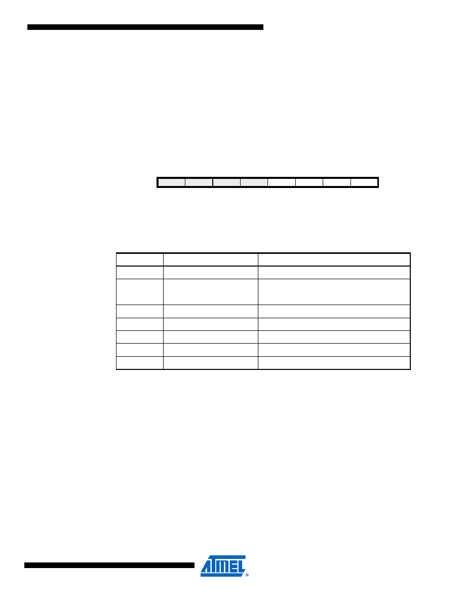
SMCR – Sleep Mode Control Register
The Sleep Mode Control Register contains control bits for power management.
Bits 3, 2, 1 – SM2:0: Sleep Mode Select Bits 2, 1, and 0
These bits select between the five available sleep modes as shown in Table 9-2.
Note:
1. Standby mode is only recommended for use with external crystals or resonators.
Bit 1 – SE: Sleep Enable
The SE bit must be written to logic one to make the MCU enter the sleep mode when the SLEEP
instruction is executed. To avoid the MCU entering the sleep mode unless it is the programmer’s
purpose, it is recommended to write the Sleep Enable (SE) bit to one just before the execution of
the SLEEP instruction and to clear it immediately after waking up.
Bit
765
4321
0
–
SM2
SM1
SM0
SE
SMCR
Read/Write
R
R/W
Initial Value
000
0000
0
Table 9-2.
Sleep Mode Select
SM2
SM1
SM0
Sleep Mode
000
Idle
001
ADC Noise Reduction
010
Power-down
011
Power-save
100
Reserved
101
Reserved
110
Standby(1)
111
Reserved
发布紧急采购,3分钟左右您将得到回复。
相关PDF资料
ATMEGA8515L-8JUR
MCU AVR 8KB FLASH 8MHZ 44PLCC
ATMEGA8515L-8PJ
IC MCU AVR 8K 5V 8MHZ 40-DIP
ATMEGA8535-16JUR
MCU AVR 8K FLASH 16MHZ 44PLCC
ATMEGA8535L-8PJ
IC MCU AVR 8K 5V 8MHZ 40-DIP
ATMEGA88-15MT2
MCU AVR 8K FLASH 15MHZ 32-QFN
ATMEGA88-20AUR
MCU AVR 8K FLASH 20MHZ 32TQFP
ATMEGA88P-20AUR
MCU AVR 8KB FLASH 20MHZ 32TQFP
ATMEGA8HVA-4CKU
MCU AVR 8K FLASH 4MHZ 36-LGA
相关代理商/技术参数
ATmega649V-8MU
功能描述:8位微控制器 -MCU AVR 64K FLASH 2K EE 4K SRAM ADC LCD RoHS:否 制造商:Silicon Labs 核心:8051 处理器系列:C8051F39x 数据总线宽度:8 bit 最大时钟频率:50 MHz 程序存储器大小:16 KB 数据 RAM 大小:1 KB 片上 ADC:Yes 工作电源电压:1.8 V to 3.6 V 工作温度范围:- 40 C to + 105 C 封装 / 箱体:QFN-20 安装风格:SMD/SMT
ATMEGA649V-8MUR
功能描述:8位微控制器 -MCU AVR 64KB FLSH 2KB EE 4KB SRAM LCD8MHz1.8V RoHS:否 制造商:Silicon Labs 核心:8051 处理器系列:C8051F39x 数据总线宽度:8 bit 最大时钟频率:50 MHz 程序存储器大小:16 KB 数据 RAM 大小:1 KB 片上 ADC:Yes 工作电源电压:1.8 V to 3.6 V 工作温度范围:- 40 C to + 105 C 封装 / 箱体:QFN-20 安装风格:SMD/SMT
ATMEGA64A-AN
功能描述:8位微控制器 -MCU 16MHz 105C RoHS:否 制造商:Silicon Labs 核心:8051 处理器系列:C8051F39x 数据总线宽度:8 bit 最大时钟频率:50 MHz 程序存储器大小:16 KB 数据 RAM 大小:1 KB 片上 ADC:Yes 工作电源电压:1.8 V to 3.6 V 工作温度范围:- 40 C to + 105 C 封装 / 箱体:QFN-20 安装风格:SMD/SMT
ATMEGA64A-ANR
功能描述:8位微控制器 -MCU 16MHz 105C RoHS:否 制造商:Silicon Labs 核心:8051 处理器系列:C8051F39x 数据总线宽度:8 bit 最大时钟频率:50 MHz 程序存储器大小:16 KB 数据 RAM 大小:1 KB 片上 ADC:Yes 工作电源电压:1.8 V to 3.6 V 工作温度范围:- 40 C to + 105 C 封装 / 箱体:QFN-20 安装风格:SMD/SMT
ATMEGA64A-AU
功能描述:8位微控制器 -MCU 64K Flsh 2K EEPROM 4K SRAM 16MHz RoHS:否 制造商:Silicon Labs 核心:8051 处理器系列:C8051F39x 数据总线宽度:8 bit 最大时钟频率:50 MHz 程序存储器大小:16 KB 数据 RAM 大小:1 KB 片上 ADC:Yes 工作电源电压:1.8 V to 3.6 V 工作温度范围:- 40 C to + 105 C 封装 / 箱体:QFN-20 安装风格:SMD/SMT
ATMEGA64A-AUR
功能描述:8位微控制器 -MCU AVR 64KB FLSH 2KB EE 4KB SRAM-16MHz IND RoHS:否 制造商:Silicon Labs 核心:8051 处理器系列:C8051F39x 数据总线宽度:8 bit 最大时钟频率:50 MHz 程序存储器大小:16 KB 数据 RAM 大小:1 KB 片上 ADC:Yes 工作电源电压:1.8 V to 3.6 V 工作温度范围:- 40 C to + 105 C 封装 / 箱体:QFN-20 安装风格:SMD/SMT
ATMEGA64A-MN
功能描述:8位微控制器 -MCU 16MHz MLF 105C RoHS:否 制造商:Silicon Labs 核心:8051 处理器系列:C8051F39x 数据总线宽度:8 bit 最大时钟频率:50 MHz 程序存储器大小:16 KB 数据 RAM 大小:1 KB 片上 ADC:Yes 工作电源电压:1.8 V to 3.6 V 工作温度范围:- 40 C to + 105 C 封装 / 箱体:QFN-20 安装风格:SMD/SMT
ATMEGA64A-MNR
功能描述:8位微控制器 -MCU 16MHz MLF105C RoHS:否 制造商:Silicon Labs 核心:8051 处理器系列:C8051F39x 数据总线宽度:8 bit 最大时钟频率:50 MHz 程序存储器大小:16 KB 数据 RAM 大小:1 KB 片上 ADC:Yes 工作电源电压:1.8 V to 3.6 V 工作温度范围:- 40 C to + 105 C 封装 / 箱体:QFN-20 安装风格:SMD/SMT